- 您现在的位置:买卖IC网 > Sheet目录368 > W9412G6IH-5 (Winbond Electronics)IC DDR-400 SDRAM 128MB 66TSSOPII
W9412G6IH
9. ELECTRICAL CHARACTERISTICS
9.1
Absolute Maximum Ratings
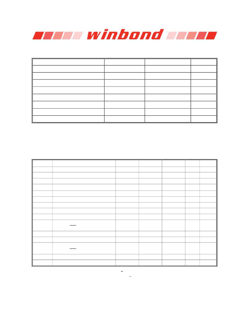
PARAMETER
Input/Output Voltage
Power Supply Voltage
Operating Temperature (-4/-5/-6)
Operating Temperature (-5I/-6I)
Storage Temperature
Soldering Temperature (10s)
Power Dissipation
Short Circuit Output Current
SYMBOL
V IN, V OUT
V DD, V DDQ
T OPR
T OPR
T STG
T SOLDER
P D
I OUT
RATING
-0.3 ~ V DDQ + 0.3
-0.3 ~ 3.6
0 ~ 70
-40 ~ 85
-55 ~ 150
260
1
50
UNIT
V
V
° C
° C
° C
° C
W
mA
Note: Stresses greater than those listed under ”Absolute Maximum Ratings” may cause permanent damage to the device.
This is a stress rating only, and functional operation of the device at these or any other conditions above those indicated in
the operational sections of this specification is not implied.
Exposure to absolute maximum rating conditions for extended periods may affect reliability.
9.2
Recommended DC Operating Conditions
(T A = 0 to 70 ° C for -4/-5/-6, T A = -40 to 85 ° C for -5I/-6I)
SYMBOL
V DD
V DD
V DDQ
V DDQ
V REF
V TT
V IH (DC)
V IL (DC)
V ICK (DC)
V ID (DC)
V IH (AC)
V IL (AC)
V ID (AC)
V X (AC)
V ISO (AC)
PARAMETER
Power Supply Voltage (for -5/-6)
Power Supply Voltage (for -4)
I/O Buffer Supply Voltage (for -5/-6)
I/O Buffer Supply Voltage (for - 4)
Input reference Voltage
Termination Voltage (System)
Input High Voltage (DC)
Input Low Voltage (DC)
Differential Clock DC Input Voltage
Input Differential Voltage.
CLK and CLK inputs (DC)
Input High Voltage (AC)
Input Low Voltage (AC)
Input Differential Voltage.
CLK and CLK inputs (AC)
Differential AC input Cross Point Voltage
Differential Clock AC Middle Point
MIN.
2.3
2.4
2.3
2.4
0.49 x V DDQ
V REF - 0.04
V REF + 0.15
-0.3
-0.3
0.36
V REF + 0.31
-
0.7
V DDQ /2 - 0.2
V DDQ /2 - 0.2
TYP.
2.5
2.5
2.5
2.5
0.50 x V DDQ
V REF
-
-
-
-
-
-
-
-
-
MAX.
2.7
2.6
2.7
2.6
0.51 x V DDQ
V REF + 0.04
V DDQ + 0.3
V REF - 0.15
V DDQ + 0.3
V DDQ + 0.6
-
V REF - 0.31
V DDQ + 0.6
V DDQ /2 + 0.2
V DDQ /2 + 0.2
UNIT
V
V
V
V
V
V
V
V
V
V
V
V
V
V
V
NOTES
2
2
2
2
2, 3
2, 8
2
2
15
13, 15
2
2
13, 15
12, 15
14, 15
Notes: Undershoot Limit: V IL (min) = -1.5V with a pulse width < 5 nS
Overshoot Limit: V IH (max) = V DDQ +1.5V with a pulse width < 5 nS
V IH (DC) and V IL (DC) are levels to maintain the current logic state.
V IH (AC) and V IL (AC) are levels to change to the new logic state.
Publication Release Date: Sep. 16, 2009
- 23 -
Revision A06
发布紧急采购,3分钟左右您将得到回复。
相关PDF资料
W9412G6JH-5I
IC DDR SDRAM 128MBIT 66TSOPII
W9425G6EH-5
IC DDR-400 SDRAM 256MB 66TSSOPII
W9425G6JH-5I
IC DDR SDRAM 256MBIT 66TSOPII
W947D2HBJX5E
IC LPDDR SDRAM 128MBIT 90VFBGA
W948D2FBJX5E
IC LPDDR SDRAM 256MBIT 90VFBGA
W949D2CBJX5E
IC LPDDR SDRAM 512MBIT 90VFBGA
W971GG6JB25I
IC DDR2 SDRAM 1GBIT 84WBGA
W971GG8JB-25
IC DDR2 SDRAM 1GBIT 60WBGA
相关代理商/技术参数
W9412G6JH
制造商:WINBOND 制造商全称:Winbond 功能描述:2M ? 4 BANKS ? 16 BITS DDR SDRAM
W9412G6JH-4
制造商:Winbond Electronics Corp 功能描述:8*16B DDR1 制造商:Winbond Electronics Corp 功能描述:IC DDR SDRAM 128M 250MHZ 66TSOP
W9412G6JH-5
制造商:Winbond Electronics Corp 功能描述:DRAM Chip DDR SDRAM 128M-Bit 8Mx16 2.5V 66-Pin TSOP 制造商:Winbond Electronics Corp 功能描述:128M BIT DDR1
W9412G6JH-5I
功能描述:IC DDR SDRAM 128MBIT 66TSOPII RoHS:是 类别:集成电路 (IC) >> 存储器 系列:- 标准包装:72 系列:- 格式 - 存储器:RAM 存储器类型:SRAM - 同步 存储容量:4.5M(256K x 18) 速度:133MHz 接口:并联 电源电压:3.135 V ~ 3.465 V 工作温度:0°C ~ 70°C 封装/外壳:100-LQFP 供应商设备封装:100-TQFP(14x20) 包装:托盘
W9412G6JH-5TR
制造商:Winbond Electronics Corp 功能描述:128M DDR SDRAM X16 200MHZ, 65N
W942
制造商:Performance Tool 功能描述:6 Piece Hook and Pick Set 制造商:PERFORMANCE TOOLS 功能描述:6 PC HOOK AND PICK SET
W942508BH
制造商:未知厂家 制造商全称:未知厂家 功能描述:DRAM
W942508CH
制造商:WINBOND 制造商全称:Winbond 功能描述:8M x 4 BANKS x 8 BIT DDR SDRAM